Business & Tech
How Small Can We Make Microchips?
Retired Intel executive describes the state of the art in computer chip technology.


Over the last four decades we have become accustomed to seeing computer chips double in capability about every two years. This phenomenon has been called Moore’s Law in honor of Intel co-founder Gordon Moore, who predicted it in 1965. On Wednesday morning retired Intel Mask Operations Manager Barry Lieberman discussed Moore’s Law and the future of lithography at Congregation Kol Emeth.
As an analogy, Leiberman showed how airplane speeds followed a Moore’s Law trend from the time of the Wright brothers until about 1960. The Concorde, the only airliner to surpass the speed of sound, was a commercial failure.
Likewise, economic considerations in computer chip manufacturing are likely to limit improvements in the speed and density of chips in a few years.
Find out what's happening in Palo Altofor free with the latest updates from Patch.
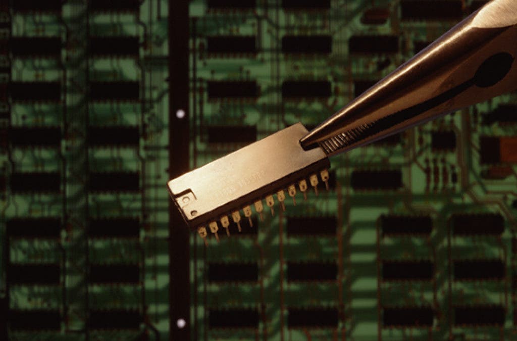
Modern computer chips are fabricated with about 30 layers of lithography. The minimum feature size (MFS) of the most advanced chips being produced in 2009 was 32 nanometers (nm). This year some chips will have an MFS of 22 nm. A 30% scaling per generation is required to justify the investment in new plants and equipment.
The chip manufacturers have been willing to make such investments in order to satisfy their customer’s demands for increased speed and density. As transistors within the chips got smaller they also got faster until power dissipation became prohibitive. So now density is the main benefit derived from reducing transistor size.
Find out what's happening in Palo Altofor free with the latest updates from Patch.
Lieberman showed how the manufacturing cost of fabricating a chip works out to about 86 cents. We’re now processing wafers that are 300 mm in diameter and may soon shift to 450 mm wafers in order to reduce the cost per chip.
He pointed out that photolithography has kept pace with the demands for reducing MFS even though resolution is limited by diffraction. There were unsuccessful attempts to replace photolithography with electron beam technology in the 1970s.
Lieberman described the currently used immersion lithography exposure tool as “a phenomenal technical achievement at 150 wafers per hour without getting bubbles.” By using water between the lens and the wafer we recover rays of light that would have otherwise been lost.
He thinks it will be possible to achieve 13.5 nm with photolithography but eventually we may have to abandon optics and go to extreme ultraviolet lithography. However, these tools are currently limited to processing only five wafers per hour. Lieberman credited Gordon Moore with having the vision to create the EUV LLC, a consortium of American chip makers devoted to developing the technology.
Lieberman regards the semiconductor industry’s innovation and generation-to-generation scaling as unprecedented and “not replicated by any other industry.” He said that optical lithography innovation has been key to this progress and none of the alternatives has ever displaced it. But marketplace power has shifted from chip companies to the customers that embed chips to create compelling end-user products and services.